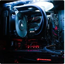
A Printed Circuit Board (PCB) is a board made of insulating material, with conductive paths etched or printed onto it. It is the physical and electrical platform that holds and connects all electronic components.
Layers of a PCB:
- Substrate (FR4) – the base layer
- Copper Layer – for conducting electricity
- Solder Mask – prevents short circuits
- Silkscreen – for labels and part IDs
Types of PCBs:
- Single-sided: Copper only on one side.
- Double-sided: Copper on both sides.
- Multilayer: Used in complex devices like phones and computers.
Design Process:
- Schematic Creation: Using tools like KiCad, Eagle, or Altium.
- Component Placement: Consider functionality, heat, and accessibility.
- Routing Traces: Signals, power, and ground paths.
- DRC Check: Ensure no violations.
- Gerber File Export: Sent to manufacturers.
PCB Design Tips:
- Keep traces short and direct.
- Use ground planes to reduce noise.
- Separate analog and digital sections.
- Pay attention to thermal reliefs.
Applications:
- Consumer electronics
- Industrial control systems
- Medical devices
- Communication systems
Mastering PCB design bridges the gap between circuit theory and real-world product development.
